Independent research laboratory — Marion, North Carolina

Advanced ceramics, and the technologies built on them.

Hardin Labs is an independent research firm founded by John F. Hardin. It develops high-performance organosilicon ceramics, and the computing, aerospace, sensing and energy technologies that follow from that one material foundation.

How to read this site

The work here is design, chemistry and simulation. Every number on this site is an engineering target or a model result, and none of it has been measured on fabricated hardware — the laboratory holds no bench of its own. Where a figure appears, the page says which it is. That distinction is the point of the lab, not a disclaimer on it.

About

One material, followed as far as it goes.

Most laboratories pick an application and then shop for a material. Hardin Labs works the other way round. It starts with a precursor chemistry — a silicon-functionalised dibenzopyran that cures and pyrolyses into a silicon-rich ceramic on a schedule the chemist chooses — and asks what becomes possible once you can place silicon deliberately in a polymer backbone and know where the ceramic will form.

The answer has turned out to reach further than expected: a circuit board that spreads its own heat, a reentry tile that sheds heat as infrared light, sensing surfaces, structural parts. They are not separate programmes that happen to share a supplier. They are the same chemistry pointed at different problems, which is why one small laboratory can credibly work on all of them at once.

What the lab does

Five areas, one foundation.

01
Advanced materials

High-performance ceramics for thermal and optical duty: precursor design, graded refractory fillers, surface veneers and the conversion chemistry that turns a polymer into a ceramic predictably.

02
Computing

Circuit substrates that carry heat, power and signal in one part — treating the board as an engineered thermal element rather than a passive carrier.

03
Aerospace

Thermal protection for reusable reentry and hypersonic flight, built around converting lattice heat into directed mid-infrared emission.

04
Sensing and life sciences

Compact diagnostic instruments and biomedical platforms built on the same ceramic and photonic primitives.

05
Energy

Cleaner fuel chemistry and energy concepts, including molecule-first engineered fuels and structural energy storage.

06
Concept work

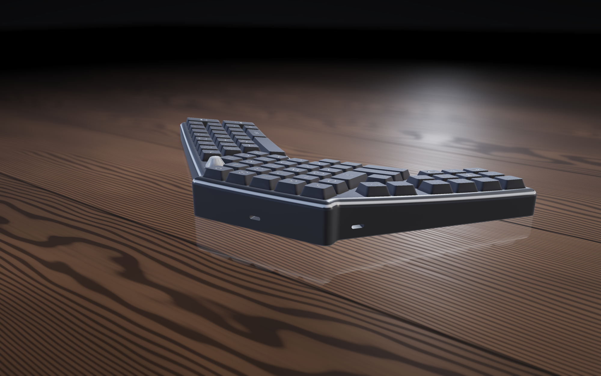
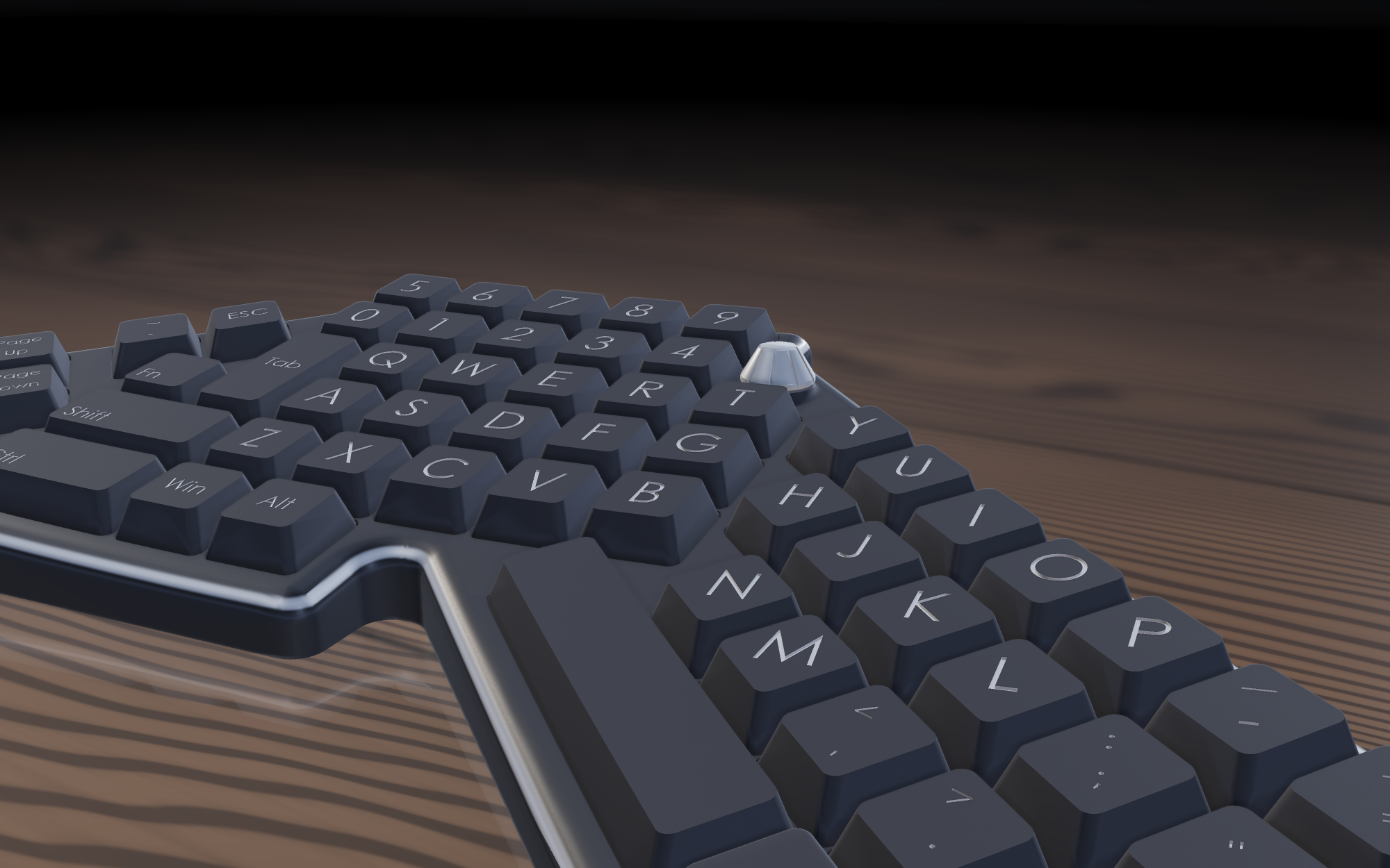
Design studies that sit outside the main programme — display architecture, instrumentation, and devices worked out on paper to see whether they hold together.

How the lab works

Chemistry first, then copper.

The rule that governs nearly every decision here: set the ceramic identity first, then add the metal. A substrate that is planarised, sealed and dimensionally settled can be plated, drilled and populated by conventional means. One that is still shrinking cannot.

Design
PrecursorSilicon placed at pendant, bridge or junction positions to program where the ceramic network forms
Convert
PyrolysisStaged under inert atmosphere: vitrification, silicon condensation, densification
Finish
VeneerPlanarisation, atomic-layer-deposited seal, then metallisation and microvias
Test
CouponsThe step the laboratory cannot yet perform in-house
Approach and philosophy

A number you have not measured is a hypothesis.

Simulation is cheap and generous. It will hand you a figure to four significant places for a material nobody has made, and the figure will look exactly like a measurement. The discipline this laboratory tries to hold is simply to keep saying which is which — to write “targets” where the honest word is targets, to name the test that would settle a claim, and to publish the counter-evidence alongside the case. One of the lab’s own reviews of surface texturing concludes that the published literature mostly argues against it; that review sits in the corpus next to the design that uses it.

The aim is not modesty for its own sake. It is that a reviewer who checks one claim and finds it hedged correctly will extend some credit to the next one. A reviewer who checks one claim and finds it inflated will not, and should not.

Current status

Where the work actually stands.

Stated plainly

No Silixon article has been fabricated. There are no coupons, no panels, no arc-jet runs and no flight tests. The evidence base is precursor chemistry reasoning, materials modelling, and one-dimensional transient thermal simulation with stated assumptions. The programme documents its own maturity as below TRL 4, with TRL 4–5 set as a goal roughly twelve to eighteen months after coupon validation begins — validation that has not yet begun.

Evidence class
ModellingChemistry design, FEA, 1-D transient conduction with declared inputs
Fabrication
None to dateFirst step is 50 × 50 mm coupons, scaling to 100 × 100 mm tiles
Nearest test
Coupon validationTGA/DSC, dilatometry, micro-CT, laser-flash conductivity, broadband dielectric spectroscopy
Constraint
Bench accessThe laboratory has no physical test capability; every measurement needs an outside facility
The work

Nine tracks.

01
Materials

The precursor chemistry itself: Sila-DBP, Siloxypyran, the conversion schedule, graded fillers and the surface veneers that make the ceramic usable.

The foundation everything else rests on
02
Computing

Silixon-PCB, Silixon-PDC and the Silixon-HCB hybrid board — a substrate that spreads heat laterally and removes it vertically, aimed at gaming, power electronics and cryogenic control hardware.

Target 120–150 W·m⁻¹·K⁻¹ in-plane · not yet measured
03
Rocketry

Thermal protection that converts lattice vibration into directed mid-infrared light through surface phonon polaritons, and sheds it through the atmospheric window.

8–13 µm emission band · modelled, never flown
04
Concept

Design studies worked out on paper: a light-field display architecture, a hovering companion device, a plasma instrument, and planetary atmospheric instrumentation.

Speculative by intent · labelled as such
05
Storage

Galinstan confined in a nanocavity, with the gallium-oxide skin that forms on it as the storage primitive. An independent device line, a clean-slate alternative, and a write-once archival card.

Built on the CRIBRUM pore membrane · nothing fabricated
06
Biosensing

The same engineered cavity asked to hold a molecule still rather than a bit. Waist geometry sets the trade between signal and access; CRUCIBLE gates it with a nanopore.

40 nm floor, 80 nm augmented candidate · modelled only
07
Photonics

Surfaces that decide how they look: metasurface skins, holographic displays, and signature management aimed at being uninteresting to a sensor rather than invisible.

Built on the nitrogen-fired optical fork · concept stage
08
Energy

A battery whose case carries load, waste heat converted rather than moved, molecule-first fuels including an off-world family, and a fusion first-wall built to be swapped in hours.

210–280 Wh/kg target · nothing built
09
Robotics

The Bioid programme — a body designed to be opened, inspected and repaired — plus the hex sensing skin and the biohybrid interface work. The longest horizon here, and labelled as such.

Virtual model only · least evidenced work on the site